Developing Bangladesh’s semiconductor workforce through educational reforms
Developing Bangladesh’s semiconductor workforce through educational reforms
Semiconductors are at the heart of humanity’s next major technological revolution, with the global market currently valued at around $575 billion. PwC projected the market to surpass $1 trillion by the next decade. Bangladesh, still in the process of being recognised as a developing country, aims to establish itself as a significant player in this sector by 2040.
Semiconductor development involves multiple stages, including silicon wafer production, chip design, fabrication, packaging, testing, and assembly. At present, Bangladesh’s role is confined to IC chip design, generating an annual revenue of about $5 million.
While high-capital processes like wafer production and fabrication remain unfeasible, the country can focus on packaging, testing, and assembly—leveraging its vast workforce.
Expanding beyond IC design could allow Bangladesh to carve out a share in the global semiconductor ecosystem, potentially generating revenues comparable to the $40 billion earned annually by the ready-made garment (RMG) sector—provided the industry receives the same strategic support.
Regionally, India now boasts 55,000 design engineers, accounting for 20% of the global chip design talent pool. In contrast, Bangladesh produces about 22,000 electrical and computer engineering graduates each year.
Experts suggest that by training just 1,000 of these graduates annually in chip design, packaging, testing, and assembly, the country could scale its semiconductor industry to $500 million within a decade. Yet, despite the sector’s strategic potential, concrete plans for workforce development through targeted education reforms remain conspicuously absent.
The current curriculum of higher educational institutes offering Electrical Engineering—the foundational domain of semiconductor studies—remains limited in its focus on this field. Only BUET (Bangladesh University of Engineering and Technology), widely regarded as the country’s most prestigious engineering school, offers a comprehensive range of semiconductor-related courses at both undergraduate and postgraduate levels.
In all engineering bachelor’s degree programmes, students must choose a final-year “concentration,” a set of elective courses designed to build specialisation. BUET’s “Electronics” group, alongside concentrations like Power, Communication, and Signal Processing, includes courses such as Processing and Fabrication Technology, Semiconductor and Nano Devices, and Analogue Integrated Circuits and Design.
At the postgraduate level, BUET significantly expands its offerings with around 20 specialised courses, including Heterostructures and Compound Semiconductor Devices and Semiconductor Characterisation Technology—essential for advanced semiconductor expertise. However, other public universities fail to match this depth and diversity.
The gap is even wider in private universities. BRAC University, currently ranked as the top private institution, offers only a handful of electives, such as optoelectronics and nanotechnology, while critical topics like characterisation techniques and IC packaging remain absent.
Similar deficiencies are seen in leading private institutions like IUB (Independent University, Bangladesh) and AIUB (American International University, Bangladesh), where key areas such as characterisation, packaging, and chip design remain underdeveloped. Compounding the issue is the shortage of expert educators in these universities.
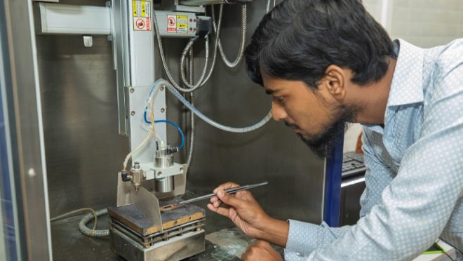
A crucial aspect of chip design and packaging is access to sophisticated laboratories and cleanroom facilities. With semiconductor miniaturisation advancing to the micro level, tools like scanning electron microscopes (SEM) and transmission electron microscopes (TEM) are indispensable.
Yet, most engineering schools in Bangladesh lack these critical facilities. Establishing such infrastructure—initially through foreign imports if necessary—is essential for developing a skilled semiconductor workforce. Without hands-on access to these tools, Bangladesh risks falling further behind in the global semiconductor race.
To address these limitations, immediate education reforms are essential to prepare a skilled workforce. Universities should introduce a comprehensive range of courses covering the entire chip lifecycle, including design, fabrication, characterisation, testing, and packaging. Beyond traditional VLSI (Very Large-Scale Integration) design courses, essential subjects like semiconductor physics, IC fabrication technology, advanced packaging techniques, device characterisation, and analogue and digital IC design should be incorporated.
These courses can be introduced as electives at the undergraduate level or as core subjects in postgraduate curricula for students seeking semiconductor specialisation. Courses on EDA tools such as Cadence, Mentor Graphics, and Synopsys, along with FPGA and ASIC design, should be offered frequently to develop expertise in chip development.
Bangladesh has semiconductor veterans working at global giants like Intel, Qualcomm, and TSMC, as well as in top academic roles. The government should offer competitive salaries, research grants, and incentives to attract these experts back to train future engineers. Universities can collaborate with these professionals to enhance course quality, ensuring students gain insights directly from industry leaders.
Additionally, sophisticated equipment such as SEM and wafer bonding tools must be acquired for hands-on learning. However, until facilities are developed, industry-academia collaborations are crucial. Universities should actively engage with local semiconductor firms to provide students access to industry labs, internships, and workshops, bridging the gap between academic learning and practical industry requirements.
For IC packaging, polytechnic and vocational training institutions should introduce hands-on courses in cleanroom management, assembly techniques, soldering, and testing protocols, focusing on practical skills without requiring deep theoretical knowledge. Government and universities should also implement exchange programs to provide students with opportunities to gain hands-on experience and exposure to advanced semiconductor technologies abroad.
These programmes could involve partnerships with leading global universities, research institutions, and semiconductor companies, enabling students to work with cutting-edge equipment such as lithography systems, cleanrooms, and advanced testing tools, which may not yet be available locally. By participating in such programmes, students can learn industry best practices, interact with global experts, and bring back valuable knowledge.
Though financially demanding, the government could establish at least one fully functional academic cleanroom facility in the capital, serving as a national training and research hub for students across the country. The government already provides incentives to IC design companies like Ulkasemi and Neural Semiconductor for component imports. These initiatives should be expanded to encourage start-ups by young student entrepreneurs, offering seed funding, mentorship, and lab access to foster innovation.
As the world marches towards a semiconductor-driven future, Bangladesh must act swiftly to reform its educational system and build a skilled workforce. Only then can it turn its aspirations into reality and secure a competitive edge in this trillion-dollar industry.

Sketch: TBS
Abrar Jawad Haque is an EU Erasmus Scholar at the Erasmus Smart Systems Integrated Solutions (SSIs).
Disclaimer: The views and opinions expressed in this article are those of the author and do not necessarily reflect the opinions and views of The Business Standard,TBS Graduates